
State-of-the-Art Epitaxy Technology
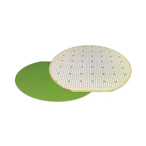
Coherent offers 100mm, 150mm, and 200mm SiC epitaxial wafers designed for applications from R&D to high-volume production. Epi specifications are customized to allow manufacturers to optimize performance and yield across various high-power and high-temperature device technologies.
Datasheet
SiC Substrates
SiC Substrates
SiC EPITAXY CAPABILITIES HIGHLIGHTS
Coherent continuously improves our materials quality and increases substrate diameters to enable our customers to increase device performance and lower costs.
Key Capabilities:
Best-in-Class Quality: High uniformity and low defects with high device yield.
- Single and Multiple: Wafer platforms with state of the art metrology tools
- Advanced Epilayers: Wide range of doping concentrations with layers up to 250 µm
- Multilayer Structures: Various doping levels, p-n junctions, embedded and contact layers
Optimized for Advanced Device Structures
Our SiC epitaxial wafers support the development of a wide range of high-performance devices, including:
- Super Junction MOSFETs
- High Voltage IGBTs
- Trench MOSFETs
- Avalanche Photo Diodes
- Particle Detectors (alpha, neutron)
These devices benefit from SiC’s material properties, making them
- Electric Vehicles
- Renewable Energy Systems
- Power Grid Distribution
- High-Temperature Industrial Applications